Applications of Tungsten Carbide Dies in the Electronics Industry
In the rapidly evolving electronics manufacturing landscape, precision tooling is a decisive factor in product quality, production efficiency, and cost competitiveness. Among advanced die materials, tungsten carbide—also known as hardmetal—has […]
In the rapidly evolving electronics manufacturing landscape, precision tooling is a decisive factor in product quality, production efficiency, and cost competitiveness. Among advanced die materials, tungsten carbide—also known as hardmetal—has emerged as the material of choice for high-demand applications in consumer electronics, semiconductor packaging, and battery production. This document examines the critical roles of tungsten carbide dies across key electronics manufacturing processes and underscores their strategic value in modern industrial ecosystems.
Material Properties Enabling High-Performance Applications
Tungsten carbide dies are engineered through powder metallurgy using tungsten and cobalt as primary constituents. This composition delivers exceptional hardness (HRA 89–94), superior wear resistance, thermal stability up to 1000°C, and outstanding corrosion resistance. These attributes enable sustained dimensional accuracy under high-pressure, high-frequency production cycles—making tungsten carbide indispensable for manufacturing micro-scale, high-tolerance electronic components where even micron-level deviations compromise functionality.
当社の工場事業:超硬部品、金型部品、医療用射出成形金型、精密射出成形金型、テフロンPFA射出成形、PFAチューブ継手。電子メール:[email protected],whatsapp:+8613302615729。
Core Applications in Electronics Manufacturing
Battery Cell Forming and Encapsulation
Tungsten carbide dies are integral to the precision stamping and sealing of lithium-ion battery cells. Their resistance to abrasive wear ensures consistent electrode alignment and seal integrity over millions of cycles, directly enhancing battery safety, energy density consistency, and production yield in high-volume smartphone and EV battery lines.
Precision Housing Fabrication
As consumer devices trend toward ultra-thin, complex geometries, tungsten carbide dies enable the replication of intricate surface textures and tight-tolerance contours in metal and polymer housings. The material’s rigidity minimizes deflection during high-speed molding, delivering flawless surface finishes and dimensional repeatability critical for premium brand aesthetics and assembly fit.
Electronic Component Molding and Machining
From micro-connectors to ceramic substrates, tungsten carbide tools maintain sub-micron tolerances during injection molding and die-cutting of passive components. Their thermal stability prevents warping under prolonged heat exposure, ensuring consistent electrical performance and minimizing post-molding rework in high-reliability applications such as automotive sensors and medical devices.
Semiconductor Packaging and PCB Assembly
Tungsten carbide push pins and alignment fixtures are essential in wafer-level packaging and surface-mount technology (SMT). These components withstand repeated mechanical stress during chip transfer and reflow soldering, guaranteeing precise placement accuracy and reducing void rates in ball grid array (BGA) and chip-scale packages (CSP). Their durability extends tool life by 3–5× compared to steel alternatives, directly lowering cost-per-unit in high-mix, high-volume fabs.
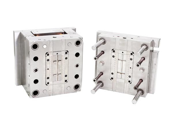
Die Manufacturing and Reconditioning
Tungsten carbide serves as both a primary die material and a repair substrate for worn or damaged tooling. Laser cladding and thermal spray techniques enable targeted restoration of critical contact surfaces, extending the service life of high-value molds by up to 70% and reducing downtime in lean manufacturing environments.
Strategic Importance in Modern Electronics Supply Chains
Tungsten carbide dies are not merely tools—they are enablers of scalability, quality, and innovation in electronics manufacturing. Their ability to sustain precision under extreme operational conditions directly supports the industry’s demands for miniaturization, higher component density, and faster time-to-market. As next-generation devices push the boundaries of thermal and mechanical performance, the adoption of tungsten carbide tooling becomes a non-negotiable competitive advantage.
FAQ
Q1: What makes tungsten carbide superior to tool steel for high-volume electronics production?
A1: Tungsten carbide offers 3–5 times greater wear resistance and maintains dimensional stability under continuous high-temperature cycles, significantly reducing tool change frequency and minimizing scrap rates in mass production.
Q2: Can tungsten carbide dies be used for both metal and plastic components in electronics?
A2: Yes. Tungsten carbide is widely employed in stamping metal housings, molding thermoplastics for connectors, and forming ceramic substrates. Its versatility stems from its hardness and thermal resilience across diverse material processing conditions.
Q3: How does tungsten carbide contribute to cost reduction in electronics manufacturing?
A3: By extending tool life, reducing maintenance downtime, and improving first-pass yield through consistent precision, tungsten carbide lowers the total cost of ownership—even with higher initial investment—delivering ROI within 6–12 months in high-volume lines.
Q4: Are there emerging trends in tungsten carbide die technology relevant to electronics?
A4: Yes. Advances in nano-grain carbide formulations and coated surfaces (e.g., TiAlN) are enhancing fracture toughness and reducing friction in micro-forming applications, enabling next-generation 5G antenna modules and wearable sensor housings.
関連記事
- Analysis of Tungsten Carbide Die Fracture Causes and Prevention Strategies
- Systematic Strategies and Practical Pathways for Extending Tungsten Carbide Die Service Life
- Environmental Impact and Sustainability of Tungsten Carbide Die Materials
- Temperature Control Technologies for Tungsten Carbide Dies: A Comprehensive Overview