Ion beam processing technology
Principles, Characteristics, Processes, and Applications of Ion Beam Processing in Microfabrication.
Principles of Ion Beam Processing.
Ion beam processing involves generating an electron beam using an electron gun under vacuum conditions. The electron beam is then introduced into an ionization chamber that has been evacuated and filled with inert gas. The low-pressure inert gas is ionized, and the resulting positive ions are extracted and subjected to steps such as acceleration and focusing. Finally, the ions are directed onto the surface of the workpiece, and material processing is achieved through the micro-mechanical impact of the ions.
The principles of ion beam processing are similar to those of electron beam processing, with the difference being that ions carry a positive charge and have a mass thousands or tens of thousands of times greater than electrons. For example, the mass of argon ions is 72,000 times that of electrons. Once the ions are accelerated to high velocities, the ion beam possesses greater impact energy compared to an electron beam. Ion beam processing relies on the micro-mechanical impact energy rather than the conversion of kinetic energy into heat for processing materials.
Our factory business: carbide parts, mold parts, medical injection molds, precision injection molds, teflon PFA injection molding, PFA tube fittings. email: [email protected],whatsapp:+8613302615729.
Characteristics of Ion Beam Processing.
Ion beam processing is a promising method for atomic and molecular-scale fabrication in microfabrication and precision manufacturing. Its characteristics can be summarized as follows:
- High processing accuracy and surface quality: Ion beam processing relies on micro-force effects for material processing, and the processed surface does not generate heat, mechanical stress, or damage. The diameter of the ion beam spot can be controlled within 1 μm, and the processing accuracy can reach the nanometer level.
- Wide range of processable materials: Since the processing takes place under vacuum conditions, it is particularly suitable for the processing of easily oxidized metals, alloy materials, and high-purity semiconductor materials.
- Various processing methods: Ion beam processing can be used for removal, coating, and implantation. These processing principles can generate a wide variety of specific methods such as shaping, etching, thinning, and exposure, which play an extremely important role in integrated circuit fabrication.
- Good performance and easy automation.
- Wide range of applications: The diameter of the ion beam spot and the energy density of the ion beam can be chosen according to the processing requirements to achieve different processing purposes. For example, a small-diameter ion beam with a high energy density is used for removal processes, while a large-diameter ion beam with a lower energy density is suitable for coating and etching. A large-diameter ion beam with weak energy is used for implantation.
- Ion beam processing requires a complete set of specialized equipment and vacuum systems, which are expensive. Therefore, its application is subject to certain limitations.
Ion Beam Processing Techniques and Applications.
The application scope of ion beam processing is expanding and continuously innovating. The main ion beam processing techniques used to modify the size and surface physical and mechanical properties of parts are ion beam sputtering removal processing, ion beam sputtering coating processing, ion beam injection surface modification processing, and ion beam projection exposure processing, as shown in Figure 1.1.
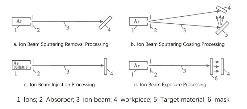
Ion Beam Sputtering Removal Processing.
Ion beam sputtering removal processing, also known as ion beam removal processing, uses argon ions with an energy range of 0.1-5 keV and a diameter of a few nanometers to bombard the surface of the workpiece. When the transmitted energy exceeds the bonding force between the surface atoms (or molecules) of the workpiece, the atoms (or molecules) on the material surface are sputtered out one by one to achieve the processing goal. It is a typical method of atomic and molecular-scale processing and ultra-precision processing.
The current main applications are as follows: firstly, machining grooves on gyro air bearings and aerostatic engines, which have high resolution, good accuracy, and consistent repeatability; secondly, etching high-precision patterns such as integrated circuits, optoelectronic devices, and optoelectronic integrated devices; thirdly, processing non-reflective textured surfaces of solar cells; fourthly, thinning materials for transmission electron microscope samples; and fifthly, processing single-crystal diamond tools, etc.
Ion Beam Sputtering Coating Processing.
Ion beam sputtering coating processing is an atomic and molecular-level deposition process, sometimes referred to as ion beam sputtering deposition. Under vacuum conditions, it uses argon ions with an energy range of 0.1-5 keV to bombard a target material, which ejects atoms or molecules from the target and deposits them onto the surface of the workpiece. On the other hand, high-speed neutral particles also impact the surface of the workpiece to enhance the adhesion between the coating and the substrate (up to 10-20 MPa). Due to the considerable kinetic energy of the sputtered neutral atoms or molecules, this coating has higher adhesion compared to methods such as evaporation and electroplating. The coating is uniform, dense, and has high efficiency.
Ion beam coating can be applied to a wide range of materials, including metals and non-metals, for depositing metal or non-metal thin films on their surfaces. It can be used for various alloys, compounds, synthetic materials, semiconductor materials, and high-melting-point materials. The applications include: coating lubricating films, heat-resistant films, wear-resistant films, decorative films, and electrical films; substituting for hard chrome plating to reduce environmental pollution; applying ion beam coating to precision ball bearings to extend their service life by thousands of hours; depositing TiN or TiC coatings a few micrometers thick on cutting tools to increase their lifespan by 3-10 times; depositing a layer of precious metal coating (such as Pt, Au, Rh) on titanium alloy blades to increase fatigue life by 30% and enhance oxidation resistance and corrosion resistance.
Ion Beam Injection Processing.
Ion beam injection processing involves ionizing the desired elements to be injected, separating and accelerating the positive ions in an electric field to form a high-energy ion beam of hundreds of kiloelectron volts, which bombards the surface of the workpiece. Due to the large kinetic energy of the ions, they penetrate into the surface layer, neutralize their charges, and become substitutional atoms or interstitial atoms in the lattice, resulting in changes in the material’s chemical composition, structure, and properties. Ion injection can be used for semiconductor material doping, metal material modification, and other purposes. The applications include: injecting impurities such as phosphorus or boron into single-crystal silicon for the production of transistors, integrated circuits, solar cells, etc.; injecting oxygen ions into iron to form Fe3O4, which improves acid resistance; injecting nitrogen ions into high-speed steel cutting tools to increase their lifespan; injecting niobium ions into tin to form NbsO, resulting in a superconducting surface, and so on.
Ion Beam Exposure Processing.
Ion beam exposure has the advantages of high sensitivity and high resolution. Since ion mass is much greater than that of electrons, it causes less backscatter and neighboring effects on the substrate, making it capable of exposing precise microstructures with linewidths below 0.1 μm. Additionally, due to the larger diameter and mass of ions compared to electrons, ions encounter greater resistance after entering the resist and have shorter range within the resist. This allows the resist to fully absorb the ion energy, resulting in increased sensitivity. Experiments have shown that when using resist, ion beam exposure has sensitivity more than one order of magnitude higher than that of electron beam exposure, allowing for significantly shorter exposure times.