electron beam processing technology
The principles, characteristics, and applications of electron beam processing technology. Definition of Microfine High-Energy Beam Processing. High-energy beam typically refers to a beam with high energy density, such as laser […]
The principles, characteristics, and applications of electron beam processing technology. Definition of Microfine High-Energy Beam Processing. High-energy beam typically refers to a beam with high energy density, such as laser beam, electron beam, plasma, and ion beam. High-energy beam processing technology refers to the use of high-energy beams for manufacturing and processing of materials or components, including welding, additive manufacturing, and surface engineering. Microfine high-energy beam processing technology is an advanced microfabrication technique that utilizes high-energy beams to induce heating, melting, vaporization, plasma, and other physical phenomena in materials, achieving purposes such as material removal, joining, growth, and modification. Due to the ability of high-energy beams to be focused to an extremely small size, with beam diameters ranging from 100 nm to 0.1 μm, and achieving processing accuracy at the nanometer level, it is a method of ultrafine processing.
Electron beam processing technology
1. Principles of Electron Beam Processing.
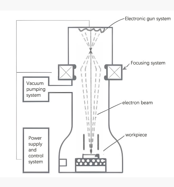
Electron beam processing refers to the emission of an electron beam from a heated cathode under vacuum conditions. The negatively charged electron beam flies towards the anode, accelerates through an accelerating electrode, and is focused by electromagnetic lenses. This results in a highly concentrated energy density, with energy concentrated into spots with diameters ranging from 0.1 to 10 μm, achieving energy densities of 10^6 to 10^9 W/cm². The high-speed impact on the surface of the workpiece converts a large portion of the energy into heat within an extremely short time, raising the temperature of the impacted material to thousands of degrees Celsius, causing melting and vaporization. The waste material generated during the impact is evacuated by the vacuum system.
Our factory business: carbide parts, mold parts, medical injection molds, precision injection molds, teflon PFA injection molding, PFA tube fittings. email: [email protected],whatsapp:+8613302615729.
1.1 Principle of electron beam processing.
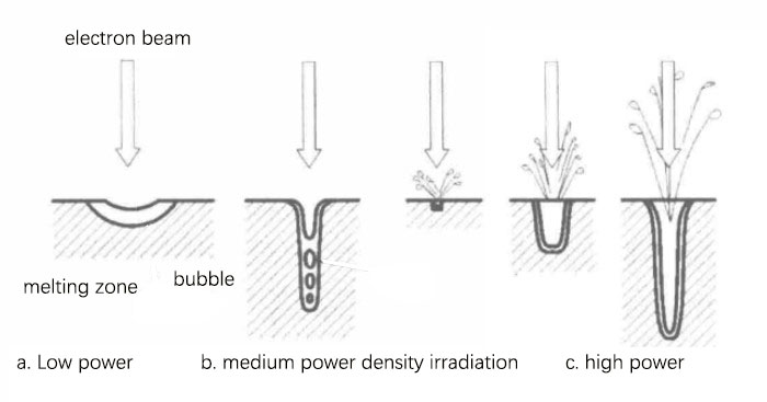
Figure 1.2 illustrates various processing techniques utilizing the thermal effects of electron beams. Figure 1.2(a) indicates that when irradiated with low power density, the saturation temperature of the central part of the electron beam is near the melting temperature. At this point, evaporation is slow and the melting pit is large, making it suitable for electron beam surface treatment to improve surface hardness and strength. Figure 1.2(b) refers to the phenomenon of melting, vaporization, and evaporation when irradiated with medium power density. If the material is transparent, some bubble-like structures can be observed, which solidify in their original state after irradiation. Medium power density irradiation can be used for electron beam welding. Figure 1.2(c) refers to the principle of electron beam drilling when irradiated with high power density. The saturation temperature of the central part of the electron beam far exceeds the vaporization temperature. Due to the pressure inside the bubbles being greater than the surface tension of the molten layer, the material is expelled from the entrance of the electron beam and effectively processed in the depth direction. This is the principle of electron beam drilling. For general metal materials, a power density of 10^6 to 10^9 W/cm² is required. In addition to drilling and grooving, high power density electron beams can also be used for the manufacture of thin film components in integrated circuitry by utilizing evaporation to obtain high-purity deposition films.
1.2 Processing using electron beams.
2. Characteristics and Applications of Electron Beam Processing.
- Electron beams have a small diameter. Electron beams can be focused to a very small size, with a diameter that can even be focused to 0.01 μm. The length of the electron beam can be tens of times the diameter, making it suitable for deep hole machining and microfine machining.
- Electron beams have high energy density. When the electron beam is focused onto a spot with a diameter of several micrometers, the energy density can reach 10^9 W/cm², sufficient to melt and vaporize any material.
- High production efficiency. Due to the high energy density and energy utilization efficiency of electron beams, the processing time for workpieces of different materials and hole sizes is generally only a few tens of seconds, even for workpieces with a thickness of about 5 mm.
- Wide range of materials for processing. Electron beam processing relies on thermal and chemical effects. The thermal influence range can be very small, and the processing is conducted under vacuum conditions, ensuring high chemical purity at the processing site. Therefore, it is suitable for processing various hard, brittle, ductile metals and non-metallic materials, heat-sensitive materials, oxidizable metals and alloys, high-purity semiconductor materials, etc.
- Minimal workpiece deformation. Electron beam processing is a non-contact machining method. During the processing, there is no obvious mechanical cutting force between the tool and the workpiece, resulting in minimal macroscopic stress and deformation. It is suitable for processing easily deformable parts.
- Easy automation. Electron beams can be quickly and accurately controlled in terms of intensity, beam diameter, and position through magnetic or electric fields, enabling a high degree of automation. It is suitable for processing circular holes, irregular holes, blind holes, tapered holesand complex three-dimensional structures.
The applications of electron beam processing technology are diverse and include.
- Electron beam welding: Electron beams can be used for high-precision welding of various materials, including metals, alloys, and dissimilar materials. It is widely used in industries such as automotive, aerospace, and electronics.
- Electron beam drilling: Electron beams can drill precise holes in materials, including metals, ceramics, and semiconductors. It is used in applications such as fuel injection nozzles, cooling holes in turbine blades, and microfluidic devices.
- Electron beam surface treatment: Electron beams can modify the surface properties of materials, such as improving hardness, wear resistance, or corrosion resistance. It is used in applications such as tool and die manufacturing, surface hardening of components, and coating deposition.
- Electron beam additive manufacturing (EBAM): Electron beams can be used in additive manufacturing processes to melt and solidify metal powders layer by layer, creating complex three-dimensional structures. EBAM is used for rapid prototyping, production of customized components, and in aerospace and medical industries.
- Electron beam lithography: Electron beams can be used in nanolithography to create patterns and structures on semiconductor wafers or other substrates with high precision. It is a key technology in semiconductor manufacturing and nanotechnology research.
- Electron beam machining: Electron beams can be used for precision machining of materials, such as cutting, grooving, and shaping. It is used in applications where high accuracy and fine details are required, such as microelectronics and micro-optics.
Advantages:
- High precision: Microfine high-energy beam processing technology can achieve processing accuracy at the nanometer level, enabling the fabrication of intricate structures and features.
- Small heat-affected zone: The focused nature of high-energy beams allows for localized heating and minimal thermal diffusion, reducing the heat-affected zone and minimizing material distortion or damage.
- Versatility: Microfine high-energy beam processing can be applied to a wide range of materials, including metals, ceramics, semiconductors, and polymers.
- Non-contact processing: The non-contact nature of high-energy beam processing minimizes tool wear and allows for the processing of delicate or fragile materials.
- High processing speed: High-energy beams can deliver a large amount of energy to the workpiece in a short time, resulting in fast processing speeds and high production efficiency.
Limitations:
- Equipment complexity and cost: The equipment required for microfine high-energy beam processing can be complex and expensive, making it less accessible for small-scale operations.
- Safety considerations: High-energy beams can pose safety hazards, requiring appropriate safety measures and controlled environments to ensure operator and equipment safety.
- Limited depth of processing: The depth of processing in microfine high-energy beam processing is typically limited due to the energy absorption characteristics of materials, which can restrict the applicability to certain applications.
- Material limitations: While microfine high-energy beam processing can be applied to a wide range of materials, the effectiveness and feasibility may vary depending on the specific material properties and characteristics.
Overall, microfine high-energy beam processing technology, such as electron beam processing, offers a powerful and precise method for manufacturing and processing materials with applications in various industries. Its ability to achieve microscale and nanoscale processing opens up new possibilities for advanced manufacturing, miniaturization, and high-precision applications.